For greater than a decade, a analysis crew at Austria’s Graz College of Expertise has been growing a way for manufacturing nanostructures with 3D geometries. In November 2023, the crew printed an article within the journal Superior Practical Supplies, documenting two main breakthroughs they’d made on that entrance.
Titled “Spectral Tuning of Plasmonic Exercise in 3D Nanostructures through Excessive-Precision Nano-Printing”, the article by the Graz crew particulars using targeted electron beam induced deposition (FEBID) to create 3D constructions from gold nanowires. Simply as considerably, the crew additionally demonstrated how they had been ready to make use of 3D simulation software program to make the method extra dependable and, due to this fact, extra repeatable.
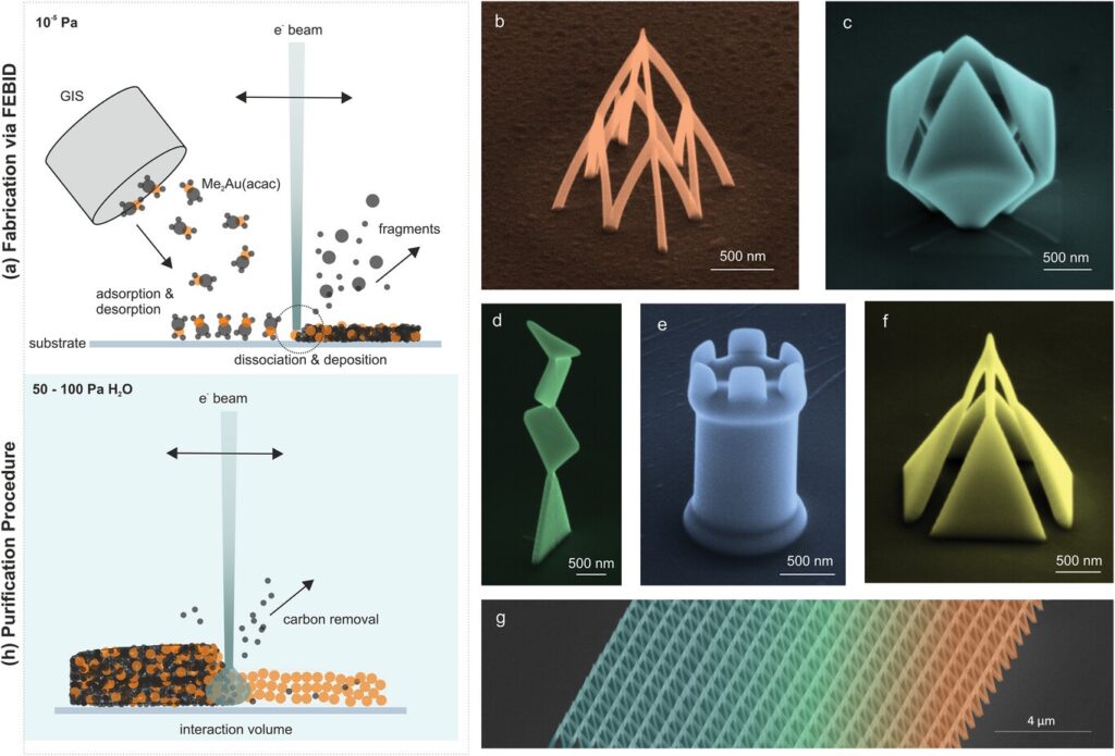
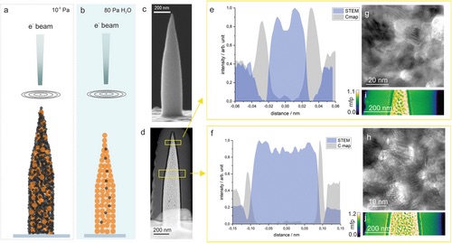
In a Graz College press launch about the breakthroughs in 3D printed nanostructures, one of many analysis leads, Harald Plank, defined, “The most important problem lately was to switch the 3D architectures into high-purity supplies with out destroying the morphology. This growth leap permits new optical results and utility ideas due to the 3D facet. By exactly controlling beam actions and publicity instances, we’re capable of produce complicated nanostructures with lattice- or sheet-like constructing blocks in a single step.” Concerning the software program facet, specifically, Plank stated, “The consistency between simulations and actual plasmonic resonances of a variety of nanoarchitectures could be very excessive. This can be a large step ahead. The onerous work of the previous couple of years has lastly paid off.”
The method works by placing a precursor materials into the vacuum chamber of a Centered Ion Beam Scanning Electron Microscopy (FIB-SEM) machine. At first, the precursor particles adhere to the chamber’s floor, after which they diffuse from each other and in the end depart the floor. Use of a targeted electron beam then yields the formation of steel deposits, with the method the crew developed permitting them to create desired 3D shapes with particular person options right down to the sub-10 nm vary.
Point out of “sub-10 nm” clearly instantly brings to thoughts the semiconductor sector, with that being the dimensions of options on probably the most superior chips at present in manufacturing. The upper the efficiency of 3D printing on the nanoscale, the extra that the 3D printing trade has to supply the semiconductor sector when it comes to purposes like superior packaging and 3D printed electronics.
It’s value noting right here that, round a month earlier than the Graz College researchers printed their outcomes, researchers from China’s Tsinghua College printed an article within the journal Science documenting their direct printing of semiconductors on the nanoscale. In opposition to this background, the timing of digital design automation (EDA) agency Synopsys’ in-progress acquisition of Ansys — stated to be largely pushed by chiplet design — turns into much more attention-grabbing.
Whereas that is nonetheless clearly very a lot an R&D utility, the semiconductor sector additionally represents maybe the quickest monitor between R&D and commercialization of any trade within the world financial system. Moreover, the truth that this particular utility already has ten years of historical past behind it suggests it might begin to be scaled up sooner slightly than later.
Pictures courtesy of Superior Practical Supplies
Subscribe to Our E mail Publication
Keep up-to-date on all the newest information from the 3D printing trade and obtain data and presents from third social gathering distributors.