It’s heady instances in energy electronics. After many years of domination by silicon, two newer supplies—silicon carbide and gallium nitride—have begun taking on multibillion-dollar markets. Silicon carbide is now the semiconductor of alternative for the inverters and chargers in electrical automobiles, for instance. And in the event you’ve bought a wall charger recently in your smartphone or laptop computer, chances are high good that it makes use of gallium nitride.
The newer supplies, generally known as wide-bandgap semiconductors, are taking on these and different power-electronics purposes as a result of they provide many superior traits. And but wide-bandgap applied sciences nonetheless have elementary weaknesses. For a silicon-carbide transistor, a giant one is comparatively low mobility of electrons within the channel—the world below the gadget’s gate via which present flows between the supply and the drain. That low mobility prevents SiC transistors from switching at excessive charges. That, in flip, limits their effectivity in purposes comparable to changing between alternating present and direct present. Gallium-nitride transistors, then again, have a quirk generally known as “dynamic on-resistance,” which implies that when the gadget is conducting present, the resistance of the gadget will depend on the voltage—greater voltage means greater on-resistance. One other drawback with GaN is that the bodily measurement of the gadget, and subsequently its price, goes up as its voltage-blocking functionality does, a big flaw for units anticipated to activate and off voltages which can be many instances greater than these discovered inside, say, a typical laptop.
What in the event you may mix GaN and SiC in a single gadget that minimizes the weaknesses of every and maximizes their strengths? That’s the query that drove a crew of 16 researchers on the Hong Kong College of Science and Expertise and three different establishments in China. After years of labor, they lastly claimed success by fabricating a transistor, which they name a hybrid field-effect transistor, or HyFET. They described their work in a paper introduced on the IEEE Worldwide Electron Gadgets Assembly, held this previous December in San Francisco.
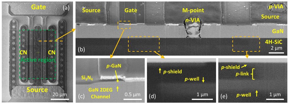 A scanning-electron microscope (SEM) picture of a HyFET, wanting down on the gadget [a], clearly exhibits the gate and a supply. A cross-sectional SEM picture of the HyFET [b] exhibits the gallium nitride transistor on the high and the silicon carbide under. Different SEM photos present the gate area of the GaN gadget [c], and the channel of the SiC transistor [d and e]. The Hong Kong College of Science and Expertise
Specialists in wide-bandgap semiconductors not concerned with the analysis have been impressed with the technical achievement. “I really am very excited in regards to the outcomes of Kevin Chen’s group in Hong Kong,” mentioned IEEE Fellow Debdeep Jena, a professor and laboratory chief at Cornell College. “It has loads of advantage and promise.” Nevertheless, these specialists’ opinions in regards to the gadget’s business prospects have been typically extra circumspect.
In operation, the gadget makes use of a low-voltage, high-speed GaN transistor to regulate a high-voltage SiC junction field-effect transistor (JFET). In a traditional SiC JFET, the drain is on the backside of the gadget, linked to the substrate. Present flows vertically, managed by a gate on high of the gadget, via a “drift layer” to a number of supply terminals, additionally on high of the gadget. Within the HyFET, that primary configuration is recognizable: There’s a drain on the backside of the gadget, linked to the substrate. Present flows upward via a SiC drift layer. Nevertheless, the gate and supply terminals are in a GaN transistor built-in straight above the SiC JFET, on the high of the gadget. So the present flowing via the SiC JFET is managed by a gate and supply terminals which can be within the GaN a part of the gadget.
The benefit right here is that it’s the GaN transistor, with its excessive electron mobility, that controls the switching of the mixed gadget. And constructed on the inspiration of the SiC JFET, with its giant drift area, the mixed gadget has the voltage-blocking capabilities of SiC. Testing indicated that the gadget largely fulfilled the researchers’ expectations. Though the mobility just isn’t fairly as excessive as for a traditional GaN gadget, it’s “appropriate for high-frequency switching,” they discovered. Additionally they demonstrated that within the “off” state, the gadget may block round 600 volts, relying on temperature—not unhealthy for a first-of-its-kind experimental gadget.
Many challenges needed to be surmounted to manufacture the gadget. One of many main ones was rising a GaN transistor straight on high of an SiC one. Gallium nitride units are routinely fabricated on substrates of SiC. Nevertheless, these units are grown “on axis,” that means they’re grown layer by layer with every layer parallel to the substrate. However SiC units are sometimes grown off axis with respect to the orientation of their substrate crystal’s lattice. So the researchers needed to devise a method of rising a GaN transistor on high of an SiC gadget with a deviance from the axis, or “miscut,” of 4 levels.
To do that they developed a way that they name two-step biaxial pressure launch. A elementary drawback with the interfaces between two totally different semiconductors is the pressure created on the boundary the place the 2 dissimilar crystals merge. This pressure can create performance-robbing imperfections within the lattice referred to as dislocations. The method refined and exploited by the researchers releases the pressure via two particular sorts of dislocations, minimizing its detrimental results.
One of many weaknesses of the HyFET is its resistance to present circulate when the transistor is within the on state. This worth, referred to as particular on-resistance (particular Ron), is sort of excessive, at round 50 milliohms – cm2. Larger Ron means decrease total effectivity. After all, the HyFET is actually the primary of its type, in-built a college laboratory.
“The big Ron in our paper outcomes from a small gadget…and a really conservative design within the SiC portion,” wrote writer and IEEE Fellow Kevin Chen in an e-mail. “Basically, there aren’t any extra obstacles towards the belief of three mΩ∙cm2 (~2.6) for a 1,200-V HyFET with industrial SiC manufacturing services.”
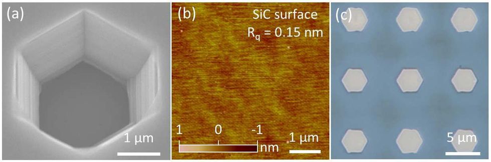 Scanning electron photos present a gap, or through, within the gallium nitride portion of the gadget [a]. When full of steel [c], these vias turn out to be conductive pathways, enabling present to circulate between the gallium-nitride and silicon-carbide parts of the gadget. A picture made with atomic drive microscopy [b] exhibits the floor of a silicon-carbide layer.The Hong Kong College of Science and Expertise
For comparability, although, a state-of-the artwork SiC or GaN transistor able to blocking greater than 600 volts can have Ron as little as 2 mΩ∙cm2, notes IEEE Life Fellow B. Jayant Baliga, the inventor of the insulated-gate bipolar transistor and Distinguished College Professor of Electrical Engineering at North Carolina State College. Given these figures, Baliga questions how a lot demand there can be for a business HyFET, when a lot easier and doubtless cheaper SiC transistors can be found. “What would encourage somebody to shift to one thing way more sophisticated, with all these layers being grown, if the particular on-resistance just isn’t lowered under that of the silicon-carbide MOSFET [metal oxide semiconductor FET]?” Baliga requested.
IEEE Fellow Umesh Mishra, Dean of the School of Engineering on the College of California Santa Barbara, and a pioneer in GaN energy units, questioned whether or not some great benefits of integrating two totally different semiconductors right into a single gadget—minuscule inductive delays and capacitive losses—have been well worth the prices in manufacturing complexity and different components. To fabricate such a tool, an organization “now has to have two applied sciences that they’re working within the fab,” he notes. “They must have silicon-carbide know-how, and so they must have gallium-nitride know-how. No one needs to do this since you now have two sophisticated applied sciences that you’re concurrently making an attempt to run”—a pricey proposition.
“To scale one thing tough is all the time arduous,” Mishra provides. “Then the query is, what’s your profit?” Mishra notes that the majority of some great benefits of the mixed gadget could possibly be obtained at a lot decrease price by merely connecting the 2 totally different transistors collectively in a single bundle, somewhat than integrating them right into a single hybrid gadget.
Writer Chen, nevertheless, advised that undesirable digital traits, notably a weak point referred to as parasitic inductance, would plague transistors which can be merely packaged collectively somewhat than built-in. “Decrease parasitic inductance minimizes switching oscillation and reduces switching loss,” he wrote in his e-mail. “Superior co-packaging strategies may cut back the parasitic inductance to a sure diploma, however is probably not as price efficient because the built-in gadget (realized in a batch course of).”
Jena, at Cornell, famous {that a} doubtlessly insurmountable impediment for the HyFET is the speed of development of GaN units, specifically. Within the foreseeable future, he says, GaN will turn out to be so succesful that it most likely gained’t require hybrid schemes to triumph. “The physics tells me that GaN is the winner in the long term,” he says. “I don’t need to take something away from the [HyFET] paper. It’s an important paper. However no matter they’ve proven right here may also be attainable with gallium nitride sooner or later,” he concludes.