Nano Dimension, through its three way partnership J.A.M.E.S, hopes to speed up the usage of 3D printed electronics. Earlier this yr, the corporate gathered customers of what it phrases Additively Manufactured Electronics at its Munich workplace the place I interviewed the attending panelists.
Dr. Filip Granek, the CEO of XTPL, an organization engaged on “deep expertise for additive manufacturing of electronics.” Granek believes printed electronics have a variety of functions, together with shows, semiconductors, superior PCBs, biosensors, and anticounterfeiting.
Their major focus is refining the decision to make options as small as “one micrometer, so roughly 100 instances smaller than the width of the human hair,” remarked Granek. XTPL’s focus is on ultra-high-resolution allotting of practical supplies, that are related to the manufacturing of electronics, together with metals, semiconductors, and isolating supplies. This leap in decision, mixed with practical supplies, is projected to unlock many functions in next-generation electronics, together with flat panel shows, superior semiconductor packaging, and bio-sensors.
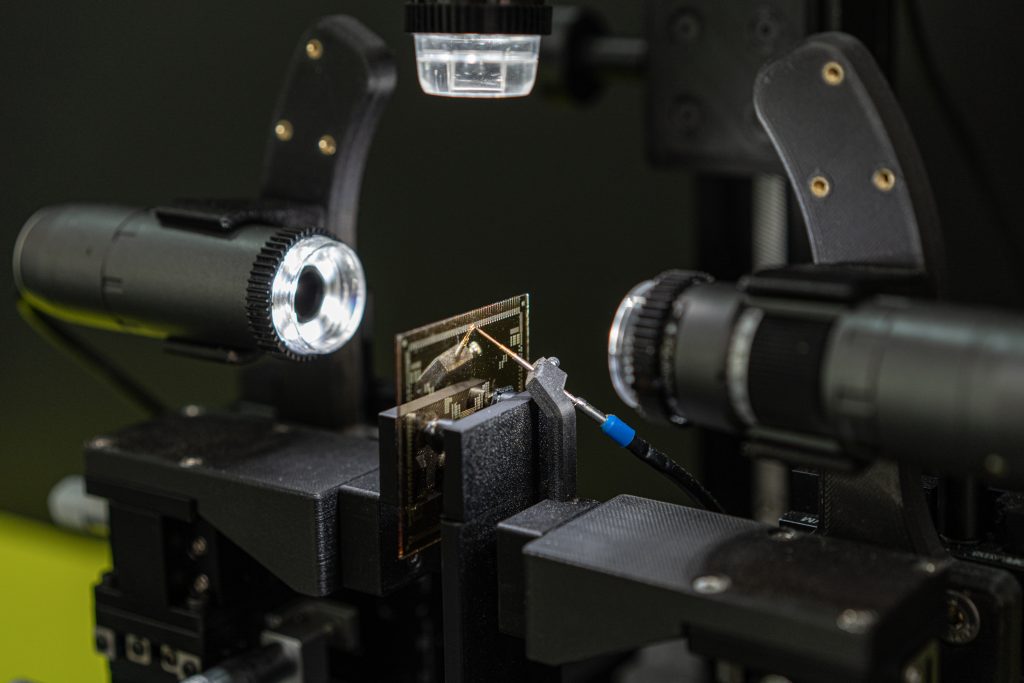
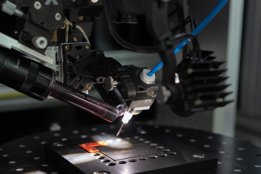
Reaching such precision isn’t any small feat. Granek defined, “Our method is on allotting. Pushing practical liquids to a really small nozzle.” He likened the method to “pushing toothpaste via a tube,” emphasizing the usage of extremely viscous inks and minuscule nozzles which can be “as small as one micrometer in diameter.”
Moreover, Granek highlighted the worth of their expertise when utilized to uncommon geometries in microelectronics. He noticed that microelectronics, at a better look, are usually not flat however have a “extremely advanced topography.” “On the microscale, direct electronics grow to be very three-dimensional,” suggesting a possible shift in how we understand and work together with electronics sooner or later. Granek underscored the problem and significance of this evolution, emphasizing the necessity to “write electrical interconnections not simply on the horizontal airplane, but additionally on a vertical airplane, with good adhesion to each layers.” This functionality, he believes, will revolutionize how we design and use digital gadgets sooner or later.
Purposes for XTPL’s printing methodology
Granek gave particulars on potential functions of their high-resolution allotting expertise within the electronics manufacturing sector. Whereas wearables and medical functions are undoubtedly among the many potential makes use of, Granek revealed the corporate’s emphasis is on “novel flat panel shows,” particularly these considerably miniaturized and supposed to be close to our eyes. Such shows not solely undertake a three-dimensional form but additionally necessitate distinctive decision. Granek additionally indicated that one other essential avenue for his or her expertise is within the “area of superior packaging within the semiconductor business,” particularly for “interconnecting particular person chips in a three-dimensional mode with a excessive decision.”
When prompted on the implications of their developments within the context of good factories or the Web of Issues (IoT), Granek acknowledged the chance however clarified that XTPL’s focus isn’t totally on end-use. As a substitute, the emphasis is on “performance within the manufacturing line.” Nonetheless, he envisages this expertise being included into “IoT or VR gadgets.” Granek additional highlighted the rising significance of bigger chips in synthetic intelligence. The growing dimension, whereas offering enhanced computational energy, necessitates perfection in each phase. He envisioned their high-resolution allotting software enjoying a pivotal function akin to a “native surgeon” in rectifying imperfections or “defects within the manufacturing line,” thereby enhancing manufacturing yield and optimizing the worth derived from these more and more costly bigger chips.
The Transition from Lab to Fab
Whereas XTPL’s ambition is reworking the world of microelectronics, its deployment takes a dual-pronged method. On the one hand, the corporate affords a “standalone R&D printer” that aids “innovators in Europe, the US, and choose main nations” of their developmental and analysis tasks. Conversely, Granek revealed in addition they possess a “printing engine” that seamlessly integrates with “third-party methods.” Collaborating intently with capital tools producers rooted deeply within the provide chains of numerous industries like flat panel show, semiconductor, and printed circuit board, XTPL goals to be an integral part of their bigger equipment.
Nevertheless, transitions include challenges. Reflecting on XTPL’s journey, Granek noticed that the corporate is at an important “turning level.” Based practically a decade in the past, the agency spent most of its years engrossed in expertise incubation. Now, as they enter the market, person suggestions — each “good” and “essential” — is shaping their course. Granek admitted the present problem lies in transitioning their expertise “from the laboratory setting into the brutal mass manufacturing setting of contemporary electronics.” Making the leap from “lab to fab” isn’t with out hurdles, however Granek’s dedication to see the corporate’s imaginative and prescient come to fruition is obvious.
Instruments and Options for Subsequent Technology Manufacturing
In charting the course for XTPL’s subsequent 5 years, CEO Filip Granek unveiled a twofold technique. In the beginning, the rapid focus lies in “closely deploy[ing] our printing modules” and fortifying partnerships with capital tools sectors. Granek envisions XTPL changing into “a acknowledged and accepted provider of high-resolution allotting options” in industries starting from flat panel shows to semiconductors and printed circuit boards. The ambition continues. Granek emphasizes XTPL’s goal to “grow to be a family identify” and envisages its integration into merchandise we’ll buy “within the subsequent 2-3-4 years in a significant market or the grocery store.”
XTPL won’t take its foot off the pedal of innovation. Granek expressed the corporate’s intent to refine its expertise, aiming for enhanced velocity and precision to cater to future-generation functions.
Granek voiced enthusiasm for international manufacturing initiatives, significantly highlighting actions just like the US’s CHIPS Act and Germany’s funding in semiconductor vegetation. He sees these actions as an auspicious signal, noting the shift in the direction of repatriating manufacturing to Europe and the US. Extra than simply establishing a producing basis, Granek views this as a possibility to bolster “innovators who create instruments and options for next-generation manufacturing.” Emphasizing the necessity for sustainable, inexperienced, and aggressive manufacturing, he believes this setting favors XTPL’s development.
Decreasing materials wastage?
Highlighting the environmental implications of semiconductor manufacturing, Filip Granek, the CEO of XTPL, sheds mild on the potential of additive processes to scale back waste and enhance effectivity. In conventional semiconductor manufacturing, the reliance on “subtractive processes” usually leads to the wastage of uncommon supplies from the Earth’s crust. Granek notes, “to provide positive options, we take away most of those uncommon supplies” solely to make the most of a fraction of them for particular functionalities.
Nevertheless, this method can change with a shift to high-resolution additive options. Granek underscores the potential of additive strategies, suggesting that “as an alternative of losing 99% of the supplies,” that are extracted with vital vitality and carbon footprint, industries can now optimize the usage of these uncommon supplies. Within the context of a quickly altering international panorama with constrained entry to sure sources, Granek believes effectivity in utilizing these supplies will acquire paramount significance.
Amid rising international considerations about useful resource constraints, Granek weighed in on China’s choice to restrict exports of two pivotal supplies. He predicted, “That is only the start of a sure international scenario we’ll face.” Granek emphasizes the rationality of optimizing the usage of uncommon supplies, particularly when a lot vitality goes into their extraction and purification. “The cheap factor to do is to not put quite a lot of effort to mine uncommon supplies after which waste most of them within the manufacturing course of,” Granek remarks, making a case for extra even handed useful resource administration.
Moreover, Granek shines a light-weight on the burgeoning function of additive manufacturing in electronics, indicating its relevance in in the present day’s evolving technological panorama. “There are a number of initiatives and a number of actions within the analysis space within the business space the place the main target of additive manufacturing within the area of electronics is changing into an actual factor,” he shares, stressing the importance of those developments for next-generation electronics.
Who’s main the business? 3D Printing Business Awards Winners.
Learn all of the 3D Printing Business protection from Formnext 2023.
To remain updated with the most recent 3D printing information, don’t neglect to subscribe to the 3D Printing Business publication or observe us on Twitter, or like our web page on Fb.
When you’re right here, why not subscribe to our Youtube channel? That includes dialogue, debriefs, video shorts, and webinar replays.
Are you in search of a job within the additive manufacturing business? Go to 3D Printing Jobs for a number of roles within the business.
Featured picture reveals a pattern made for Taiwan’s Industrial Know-how Analysis Institute. Picture through XTPL.